Integrated Circuit Design & Testing
Senseeker offers a range of services from IC design, testing and qualification to foundry management. Specializing in state-of-the-art mixed-signal technology, Senseeker's products and IP enable our customers to produce cutting-edge infrared image sensing and transduction solutions that outperform all other commercially available solutions.

Integrated Circuit Design
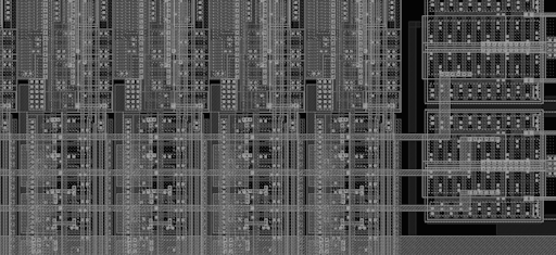
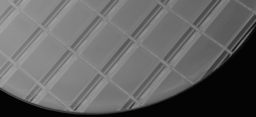
Senseeker has extensive experience in designing cutting-edge DROICs that enable state-of-the-art infrared imaging systems. These DROICs have been fabricated in multiple CMOS wafer fabs at different processing geometries. Senseeker has vast experience with all aspects of DROIC design and has a library of proven IP that can be leveraged to accelerate a custom design and ensure that IC performance targets are met.
DROICs for infrared and other 3-D stacked image sensors
Pixel-parallel solutions
Column-parallel conversion
14+ bit column-level ADC arrays and associated digital video processors in single-digit µm pitch
Staring arrays and scanning linear formats
High resolution multi-megapixel formats
High frame rate data transmission
Readout pixel designs
Pixels pitch down to just a few micrometers
Single color, 2-color, multi-color and hyperspectral
Digital pixel sensors including delta-sigma modulation (DSM), pulse-frequency modulation (PFM) and slope algorithms
Detector bias methods such as direct injection (DI), buffered direct injection (BDI) and capacitive transimpedance amplifiers (CTIA)
In-pixel background removal or addition, manual and automated self-measured compensation
Correlated double sample (CDS) and sub-frame averaging (SFA) filters
Standard interface formats
SenSPI
Standardized outputs and serializer formats for direct communication to commercial frame grabbers
Individual serializers with data rates in excess of 20 Gbps
High dynamic range digital pixel readouts
Megapixel-class HDR digital pixel architectures
Very low power compared to conventional digital pixels
On-chip data calibration and real-time processing
Select linearization routines
Foreground and background calibration of image sensor ADC data
Bad pixel replacement and data manipulation
Thresholding and motion vector identification
Radiation tolerant designs
Single-event effect (SEE): Rejection with triple modular redundancy (TMR) at the architecture level and lower
Total ionizing dose (TID): Heavily hardened designs beyond that possible with shallow trench isolation (STI) using enclosed geometry transistors and guard rings
Large stitched designs
>>100 Mpixel possible
Example: 67 Mpixel designs with frame rates > 60 fps at 14-bit resolution
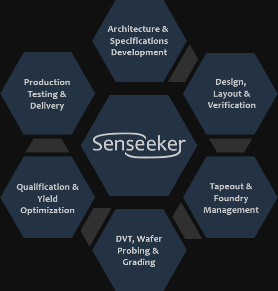
Circuit Design
Schematic Entry
Layout & Verification
Tapeout & Fabrication
Foundry Management
Customer-managed foundry model
Complete custom design
Senseeker's best-in-class IP available off-the-shelf if required
GDSII database and GDSII layer list delivered to customer
Customer manages foundry directly and has exclusive rights to the IC
Senseeker-managed foundry model
Same flow as custom design but Senseeker will manage product qualification, test, yield optimization and delivery
Consider this option as an exclusive custom product IC that will be available to you off-the-shelf
Foundry partners
Senseeker products are manufactured in industry leading wafer fabs located in the United States. The CMOS process geometry that is implemented supports high-yielding wafers and exceptional product life. Our manufacturing partners include onsemi, SkyWater Technology and Tower Semiconductor.


Integrated Circuit Testing
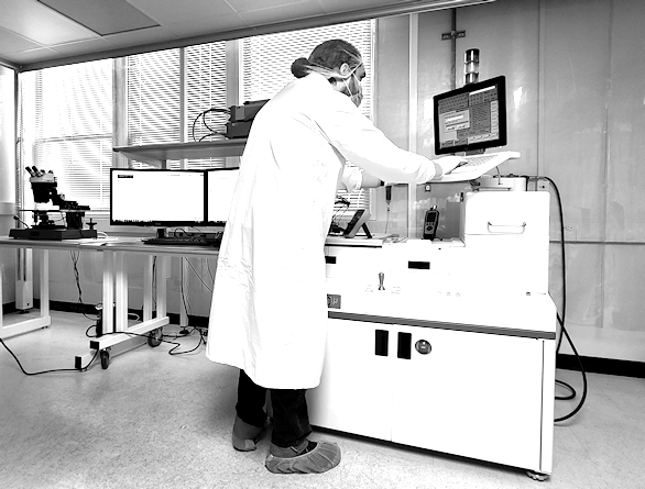
The Senseeker facility in Santa Barbara includes a Class 10,000 cleanroom equipped with a wafer probe station. This capability enables Senseeker to respond to customer demand quickly with on-site testing and also allows new silicon to be verified quickly. The Electroglas 4090u wafer prober provides fully-automated state-of-the-art die probing capability. Our dedicated test team has tested die, partial wafers and full wafers in this cleanroom environment. Industry standard test methods are complemented by advanced built-in self-test (BIST) circuits to accomplish IC performance verification with speed, precision and accuracy.
Class 10,000 Cleanroom
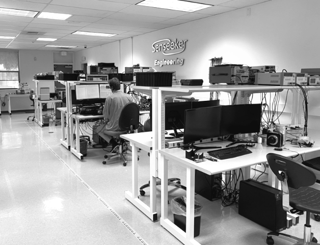
Test Lab
The Senseeker test lab is equipped to perform testing from semiconductor dies to assembled ICs under an extreme range of conditions, including cryogenic and high-temperature oven testing. In addition to reducing wafer delivery cycle times, Senseeker is equipped to support specialized customer test, failure analysis and manufacturing yield enhancements.
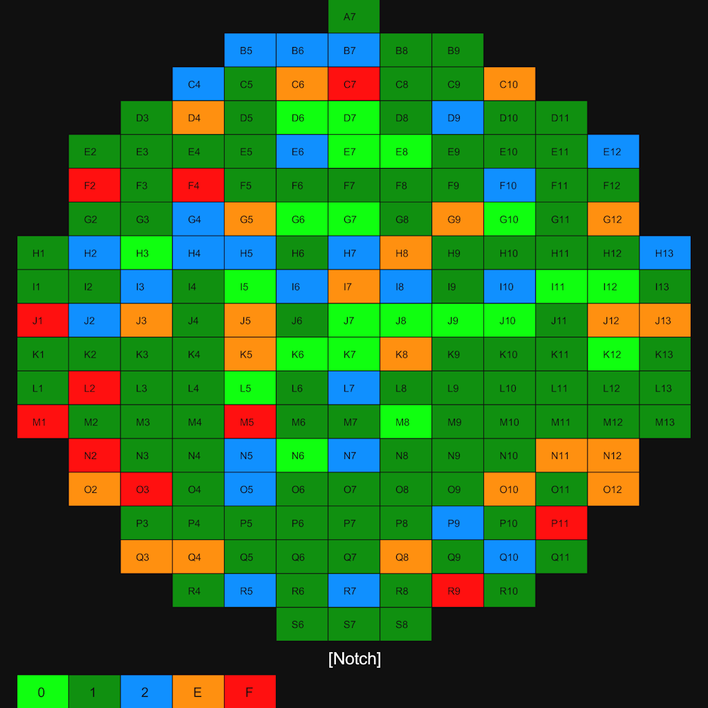
Senseeker products are delivered to customers fully tested, graded and accompanied with wafer maps detailing the characteristics of each die. When wafers are shipped to customers, Senseeker provides an executable GUI that runs on a PC to share detailed die test data for each wafer. The GUI opens up to an image of the wafer that illustrates the 'grades' of die through color coding. Clicking on any individual die on the wafer image will open another screen that provides a dashboard of electrical test characteristics for that particular die. This includes test images of the array, histograms with test limits, measured supply currents and a succinct breakdown of pass/fail conditions based on the test criteria. It is even possible to drill down further by selecting individual pixels in the array.